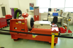
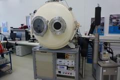
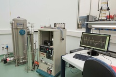
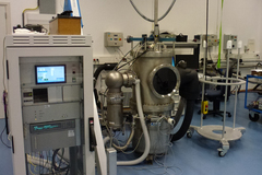
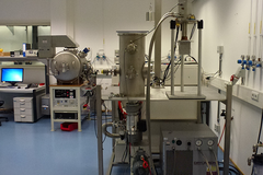
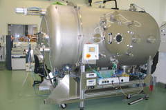
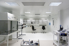
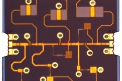
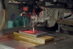
Since 2021, SERMA MICROELECTRONICS offers through its subsidiary TFP (Thin Film Products) custom thin film ceramics circuits production. In house sputtering technique combined to photolithography and photo-etching process allows TFP to produce on demand, and in fast turnaround, circuits for various hi-rel applications (Microwave, laser, photonics,…)
Type:
Service
Available standards (e.g. ASTM, MIL):
MIL, SPACE
Specimen length [mm]:
100.0
Specimen width/dia [mm]:
100.0
Specimen height/thk [mm]:
1.06
Mass max. [kg]:
0.0
Cleanroom classes (ISO 14644-1):
ISO Class ≤5
ISO Class 6
ISO Class 7
ISO Class 8
ISO Class 9
Keywords:
Thin film microwave circuits photonics TFP sputtering PVD