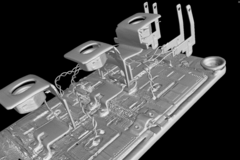
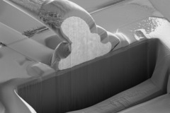
ELEMCA provides CT-scan (computed tomography: 3D X-ray imaging) on a wide array of EEE devices: semiconductor components (MEMS, sensors, discrete), passives, assembled boards and integrated module.
Your needs
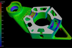
- defect localization (check our turn-key solution for Failure analysis https://triasrnd.com/en/l/418-failure-analysis )
- integrity verification (solder joints, package sealing, die attach, internal wire-bonding...)
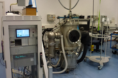
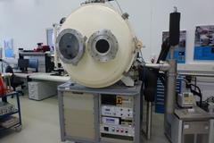
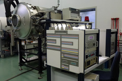
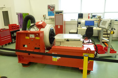
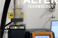
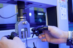
Our NDT engineers & technicians team use a very high-resolution CT-scanner (RX solutions), tailor-made for semiconductor components and chips.
key features
ultimate resolution < 5µm
laminography mode (for large PCBA)
Our space industrial customers (OEMs, payload suppliers), EMS and semiconductor IDMs appreciate ELEMCA key advantages:
-fast-delivery
-cost-competitive rates
-clear localization of potential defects
warning EEE parts exposure to X-ray may induce unexpected faults, especially on discrete components and ICs.