ELEMCA provides Failure analyses on various EEE devices: semiconductor components (MEMS, sensors, discrete), passives and assembled boards, especially solder joints.
Your needs
- design debug
- manufacturing issue (yield, process shift)
- operation failure: 0km or field return
Our PhD & engineers team applies a flexible step-by-step method, to localize, characterize and identify the origin of the defect you encountered, called "root cause".
ELEMCA workflow: Failure Analysis
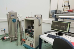
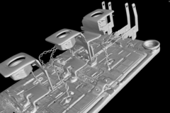
Electrical tests, at board-level or component-level (probing or device extraction): failure mode recording (i.e. "how the device lost its functionality ?")
External visual examination
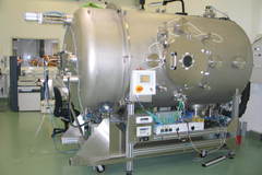
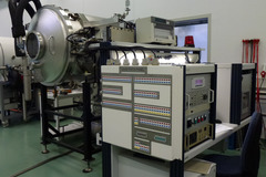
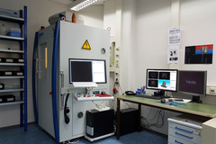
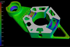
Non-destructive localization of the defect, by 3D X-ray Computed Tomography or, for dissipative thermal defects (hot spots), LIT (IR Lock-In Thermography)
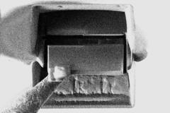
Access to the defect area: package opening or microsection
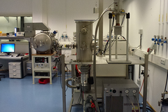
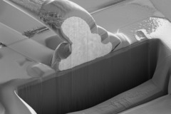
Physical & chemical characterization (SEM / STEM / TEM + EDS / EBSD) of the defect: chemical composition, morphology, microstructure, fractography...
Our space industrial customers (OEMs, payload suppliers), EMS and semiconductor IDMs appreciate ELEMCA key advantages:
- fast-delivery
- cost-competitive rates
- comprehensive & clear diagnosis : root cause identification + (when applicable) recommendation of corrective actions