SERMA Technologies offers a wide range of services in microstructures analyses for EEE parts up to the atomic scale:
Optical microscopy
-Optical microscopes with digital camera (1600x1200 pixels) and Axon software (Newtec)Scanning Electron Microscopy (SEM) allows to obtain chemical and textural information (conventional and high resolution SEM coupled to EDX analysis).
-MEB ZEISS Gemini 1530 - SE and BSE detectors; EDX
-MEB ZEISS Gemini Ultra 55 - SE et BSE detectors; STEM; EDX
-MEB Hitachi 5500 – SE detectors; STEM; EDX
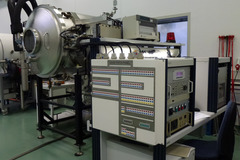
-Dual Beam STRATA 400 FEI equipped with a FIB column and a SEM column
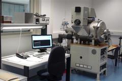
-Dual Beam NVISION 40 ZEISS equipped with a FIB column and a SEM columnTransmission Electron Microscopy (TEM) provides information on the texture (size, objects morphology, surface roughness and interfaces), structure (phases and crystalline orientations: electronic precession) and composition (X signal analysis by EDX, energy losses EELS).
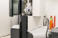
-TEM TECNAI G2 F20 S-TWIN from FEI - 200kV; STEM BF and HAADF; EDX
-TEM TECNAI OSIRIS from FEI - 80kV à 200kV; STEM BF, DF2, DF4, and HAADF; EELS filter (Type GIF); EDX (4
Super-X detectors with SDD technology)
-TEM JEOL JEM-2010FEF - 200kV; STEM BF and HAADF; ASTAR system; EELS filter (Type Ω)
Getting access to information about the physico-chemical mechanisms is critical determining the root cause of a failure such as corrosion, adhesion, oxidation, diffusion, implantation, strain…
SERMA Technologies services at a glance: failure analysis, dimensional analysis, crystallographic analysis, elemental analysis, 3D visualization of a micrometric object.